|
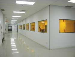
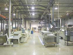
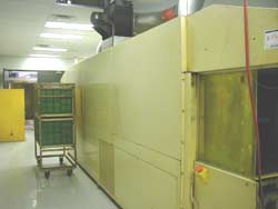
Milplex's new facility
has allowed us to create a modern layout that
reduces work in process and facilitates workflow. At
the same time we included the best technology in
clean rooms and work environments.
|
|
 |
|
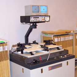 |
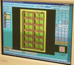
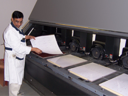
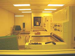
Engineering & Artwork generation:
The first step in
the manufacturing of a new product is the CAM
engineer stage. Milplex uses the most advanced
software available today on the market, GENESIS
2000.
This tool permits a
detailed "Design Rule Check" which can often catch
problems before they are manufactured.
The next stage is the generation of production
artwork.
This is done in our
class 10,000 clean room, with in-house photo
plotting and the latest Multiline tooling system.
|
|
|
|
Multi-layer:
The first step in
the production cycle of a multi-layer board is the
inner layer process. Etched layers are inspected
using modern automated inspection systems.
After inspection the
layers are oxide coated using a special horizontal
oxide replacement process.
The final steps
include post etch punching (tooling), lay-up, and
lamination in our state of the art multi-layer
department
|
|
|
|
|
|
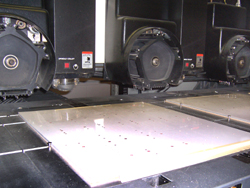
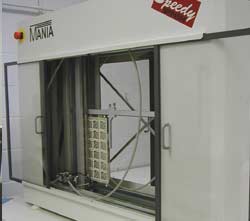
Drill
& Routing Department:
Milplex has state of
the art drilling equipment allowing us to drill
small holes and do control depth drilling.
We are able to do
standard routing of individual boards and customer
pallets.
We are also able to
offer scoring as an alternative or in combination
with routing.
|
|
|
|
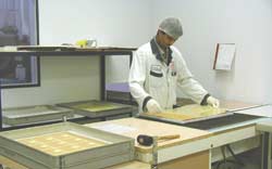
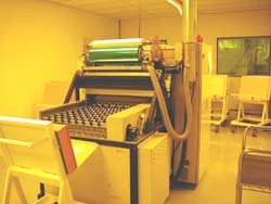
Imaging Department:
Our imaging
department is part of our class 10,000 cleanroom
complex that includes
- Art work generation and inspection
- Dry film lamination
- Dry film imaging
- Solder mask imaging
Printed circuit
panels are brought in to the department and first
laminated with dry film using modern cut sheet
lamination equipment.
This process
minimizes the amount of film used and improves
quality, and is the most cost effective method
available today.
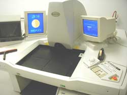
Panels are then
imaged using glass frame tooling to achieve high
productivity and accurate registration.
|
|
|
|
|
 |
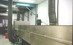
Wet
Process Department:
The wet process
department includes,
- Desmear & Electroless copper line
- Copper and tin plating
- Nickel and gold tab plating
- Chemical precleaning
- Hot air leveling
In fact all wet
chemical processing is carried out in this
department. This is the physical hub of the building
and therefore is also the center for the sequence of
processes that make a printed circuit board.
|
|
|
|
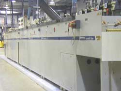
Solder Mask Department:
Various solder
masks, silk screens, carbon, and peelable masks are
applied in this department. The main activity is the
application of solder mask, which is accomplished
using an automatic spray line. This line guarantees
uniform mask application, with the highest through
put and productivity.
After the mask is applied, the image is produced by
photo imaging in the solder mask imaging section of
our clean room complex.
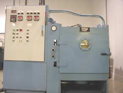
The final step is
thermal curing done in a continuous process oven,
which minimizes handling and warpage. |
|
|
|
|
|
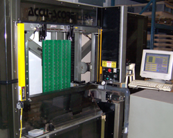
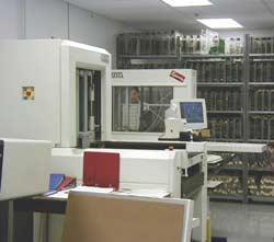
Electrical testing Department:
One of the most
important steps today is electrical testing.
It is insurance for
the customer, that he will receive functional
products and avoid the costly assembly of defect
products.
Milplex's test
department can handle almost any technology
challenge with our wide range of testing equipment.
With both single
sided and double sided test equipment we are able to
handle testing surface mount and ball grid arrays.
For prototypes we
have flying probe test equipment, which eliminates
the need for expensive permanent fixtures when the
design is not yet finished.
|
|
|
|
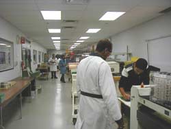
Inspection & AQL Department:
Final inspection and
AQL are the final steps at the end of processing to
insure that only quality products are shipped to our
customers.
All our printed
circuit boards are built and inspected to IPC 600
class 2 as a minimum standard. We also build to
other specifications if required by a customer. |
 |